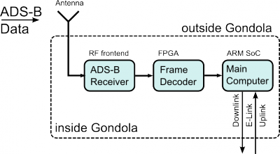
In the picture below, the three main electronic components are outlined. The ADS-B receiver is in testing at the moment, the FPGA-Hardware schematic is finished and the main computer is shown further down the page. The Antenna will be a collinear antenna of 7 to 10 segments and will be shown here, soon.
As a primary goal of our experiment is NOT to rely on commercial products (where possible), but instead develop our own system.

Electronic concept
RF front end
The first design of the RF receiver and demodulator used the well-known and often-used “miniADSB” circuit. As it proved not to be working well enough under BEXUS operating conditions (heavy oscillation, leading to reduced input sensitivity), we redesigned it to fit our needs.
It now consists of an input SAW filter tuned to 1090 MHz with low insertion loss (2.3dB), an amplifier stage (15dB), followed by another filter (2.3dB) and yet another amplifier (15dB) feeding into the final filter and detector to demodulate the (On-Off-Keying) amplitude modulation. The achieved goal of splitting the high input gain of the first design (35dB) into two amplifiers is that the system does not oscillate anymore, because feedback into the sensitive LNAs is reduced. The demodulated data is low-pass filtered and brought into the digital domain by a 16MS/s ADC.

RF front end prototype
FPGA
The FPGA board is actually under development. It will consist of an Altera Cyclone IV FPGA.
It’s goal is to do the necessary signal processing to decode the ADS-B signal. It filters noise and interference from the received signal and only transmits the correctly decoded frames to the embedded ARM computer.
ARM-computer
Here is one of the first pieces of the finished hardware: Hannes’ ARM9 embedded computer. This small computer was developed as Hannes Master thesis with the focus on low power consumption and reliability.
With an external board it can be equipped with an Ethernet PHY for connection to E-Link and will be connected to the FPGA (see below).
The ARM9 computer will be running with a small Linux kernel.

ARM9 board
Power supply
The experiment will get 28V from the BEXUS gondola. This voltage will be downconverted to a intermediate voltage of 5V.
On the ARM board, 1.0V, 1.8V and 3.3V are needed. 3.3V and 1.0V can be used as the I/O and core-voltages of the FPGA, as well as the 3.3V supply for the Ethernet PHY, the ADC and the RF receiver. The FPGA needs one more voltage for the analogue PLLs, which is 2.5V. It is generated by a LDO regulator directly on the base board.
All in all, the ARCA experiment will consume a power of less then 1W.

Power supply